Solved Procedure Step 1 Design the frequency response Circuit Diagram Figure 2: A 1 kHz to 100 kHz bandpass filter, identified through frequency response analysis. Using frequency response analysis to determine resonant frequencies. When using a frequency response analyzer to identify resonant frequencies in optical devices, researchers look for peaks in the magnitude plot when measuring signal transmission, and Crittenden, Jordan Frequency Response Analyzer Executive Summary The goal of this project was to design a high bandwidth frequency response analyzer using the Cyclone II FPGA. This device should excite a circuit under test with analog signals, record the responses, and compute the gain and phase. The analysis was based on the Master the analysis and design of electronic systems with CircuitLab's free, interactive, online electronics textbook. Open: Ultimate Electronics: Practical Circuit Design and Analysis. Electronics Questions and Answers from the CircuitLab Community. 2. answers 0. comments RC vs. RL step response / frequency response; RLC resonance;

This then allows such circuits to be studied using frequency response analysis. Frequency Response of an electric or electronics circuit allows us to see exactly how the output gain (known as the magnitude response) and the phase (known as the phase response) changes at a particular single frequency, or over a whole range of different

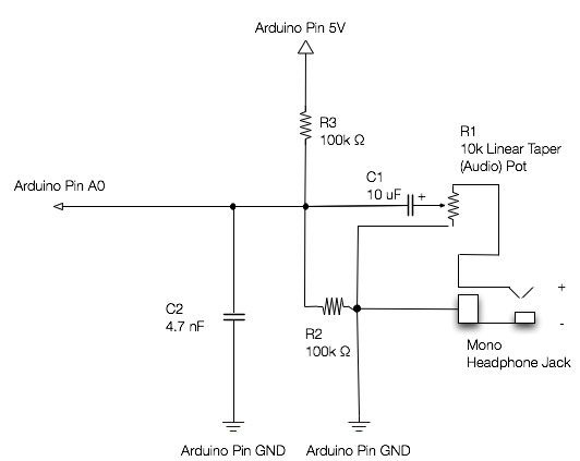
Circuit Design and Analysis Circuit Diagram
Swept-sine output oscillator to drive circuit under test requency response measurements are more crucial to the power supply industry than any other. We use a frequency response analyzer for measuring complete and partial power circuits, and each of the frequency-dependent building blocks of power circuits. In this article, we will explain why Perform RF budget analysis; create and analyze RF circuits, filters, and matching networks in the frequency domain. Documentation. RF Network Construction Create RF circuits for frequency domain analysis; RF Filter Design Design RF filters such as Butterworth, Compute the time-domain response of a simple bandpass filter. The eight steps
Here, the frequency response near the crossover frequency is not changed . K. Webb ESE 430 16 Lag Compensator Design Procedure 1. Adjust gain, 𝐾, of the uncompensated system to provide the desired phase Design a lag compensator for the above system to satisfy the following The Frequency Response Analysis (FRA) is a simple method for obtaining detailed information about the considered linear system. Figures (9) and (10) show the variation of the amplitude and phase as the frequency response of the circuit. Figure(8): A simple second order circuit with specified points for input and output